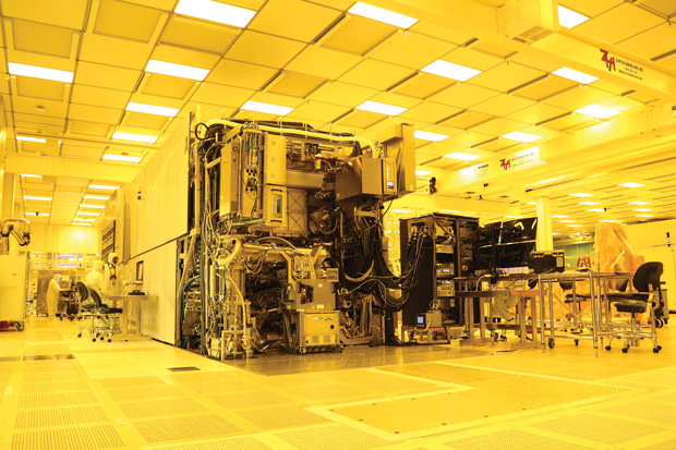
TSMC announced that it has started to provide risk production by completing its manufacturing infrastructure with 5nm manufacturing process.
The wiring width when the semiconductor circuit is manufactured into a wafer is referred to as a manufacturing process. As the minimum machining dimension becomes smaller, more transistors and wirings can be arranged in the same area. Therefore, it is possible to realize semiconductor high-speed operation.
The 5-nm manufacturing process, which TSMC has released with its design board, can achieve memory and power optimizations at 1.8-times the transistor density and 15% speed increase compared to the company’s 7-nm manufacturing process in extreme ultraviolet lithography EUV. TSMC plans to provide the 5nm manufacturing process with the main target of the growing 5G mobile market and AI market.
TSMC started this time because it is dangerous to start production without receiving a customer request, and it takes more time until products with 5nm manufacturing process actually come on the market. Apple, which is commissioning semiconductor production to TSMC, is likely to mount a 5nm manufacturing process chip on the 2020 model iPhone. TSMC also aims to realize a 3nm manufacturing process in 2022. For more information, please click here .

