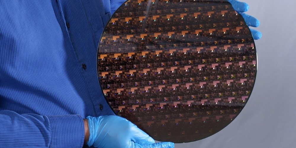
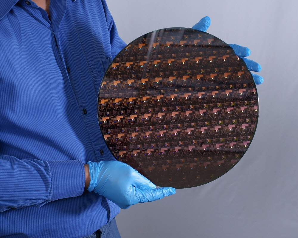
IBM announced on May 6 (local time) that it has produced the world’s first 2nm manufacturing process chip using its nanosheet technology. The development of chips for the 2nm manufacturing process is important in the semiconductor field and is expected to have a great impact on computers, communication devices, and space development.
As cloud, AI, and the Internet of Things are important, the demand for improved chip performance and energy efficiency is increasing. However, in recent years, Moore’s Law, which states that semiconductor density doubles every two years, has been broken, and in 2017, the president of TSMC, a semiconductor foundry, said that Moore’s Law is no longer valid.
Meanwhile, IBM, which succeeded in producing 5nm manufacturing process in 2017, announced that it produced a new 2nm manufacturing process chip. Semiconductors are in charge of computing core and are an important component in various fields such as electronic products, smartphones, and transportation systems. The larger the number of chip transistors, the more operations can be performed with the same power. A number of transistors are lined up on a silicon wafer, which is like a high-tech cookie sheet. IBM succeeded in developing the world’s first 2nm manufacturing process chip based on the technology that made the 5nm manufacturing process chip in 2017, four years ago.
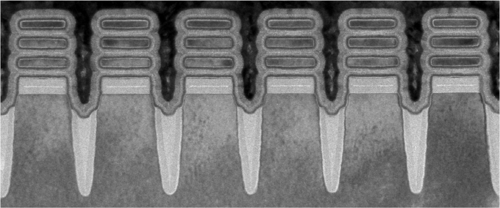
Transistors manufactured by the 2nm manufacturing process are smaller than DNA strands. The semiconductor research facility in Albany, New York, where IBM manufactured the 2nm manufacturing process chip. With the success of the 2nm manufacturing process chip, 50 billion transistors can be put on a 150mm 2 wafer, the size of a fingernail, and the transistor density reaches 333 million per 1mm 2.

Due to the improved semiconductor integration, the 2nm manufacturing process chip has various advantages over the past. For example, a 2nm manufacturing process chip is expected to perform 45% higher than a 7nm manufacturing process chip, and the same performance processor energy consumption is expected to decrease by 75%. This indicates the possibility that the battery life of smartphones, etc. will be extended by 4 times.
In addition, there are potential advantages such as reduction of carbon dioxide emissions in data centers, language translation by speeding up laptop computers, improvement of Internet, etc., detection of objects in autonomous vehicles, and improvement of response time. Not only that, it also helps to promote advances in AI, 5G autonomous systems, and space exploration.
The 2nm manufacturing process chip development utilizes the know-how that IBM has accumulated in the 5nm manufacturing process and 7nm manufacturing process development. IBM says that IBM itself will not manufacture chips for the 2nm manufacturing process, but will use partners including Samsung Electronics to manufacture processors. In the next three years, IBM plans to improve its 2nm manufacturing process and fix potential defects. It explains that a tremendous effort is required from here to production. In addition, it is revealed that TSMC is conducting research and development in addition to IBM to develop the 2nm manufacturing process. Related information can be found here.


Add comment